The Nano Dimension dual-material inkjet DragonFly 2020 3D printer creates professional multi-layer printed circuit boards that include vias, without the need for drilling. The equipment deposits both dielectric and conductive inks and performs an integrated sintering process for curing both materials. Image courtesy of Nano Dimension.


Latest News
February 1, 2016
 The 3D-printed BOOMcast was custom-created by FATHOM design studio to support Mike North’s broken leg and supply electronic sensor information via Wi-Fi to North’s doctor. As a bonus, the cast includes a Bluetooth sound system and LED sensor-feedback lights. Image courtesy of FATHOM.
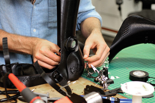
Last year may have been the Year of Electronics 3D printing, as evidenced by activity with conductive inks, conductive plastics, conformal surface-deposition and multi-material 3D design. The building blocks for 3D-printed/3D structural electronics are popping up across a wide spectrum of cost and applications, from F-Electric conductive filament offered by Functionalize to direct-printed sensors made possible by Optomec’s Aerosol Jet systems. This month, DE takes a look at grad students, individual innovators, system manufacturers and industry giants who are all contributing to this latest evolution in additive manufacturing (AM).
The Mother of Invention
Sometimes the coolest product ideas come from everyday frustrations. How often do you grab a milk carton from the refrigerator and pour a glass, only to have the first sip tell you the milk is spoiled? That scenario inspired the SmartCap, a demonstration of 3D-printed sensor technology by Liwei Lin and his students at the Berkeley Sensor and Actuator Center at University of California, Berkeley.
The proof-of-concept SmartCap (tested on a milk carton) was built on a dual-nozzle 3D Systems ProJet HD 3000, with alternating regions of polymer and sacrificial materials. By melting out the latter material and injecting the resulting tunnels with conductive metal paste that hardened, the team created an inductor-capacitor circuit with two electrodes separated by an air gap. Tilting the carton filled the gap with milk, whose dielectric constant determined the resonant frequency of the circuit as connected to a network analyzer. As the milk aged, bacterial growth changed the dielectric constant and shifted the measured frequency. Lin says the technology could have many applications in the health field.
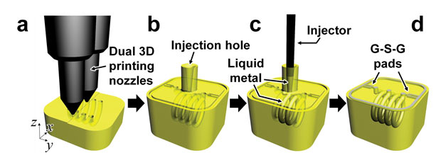
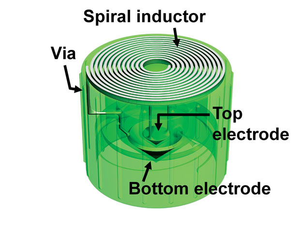
 Diagrams and elements of the SmartCap, a 3D-printed device that incorporates conductive metal traces to form an LC filter/spoilage sensor. When fluid such as milk enters and fills the capacitive gap, its changing properties (as the milk spoils) affect the resonant frequency of the filter, which can be electronically monitored. Image courtesy of Berkeley Sensor and Actuator Center, University of California, Berkeley.
Sensors embedded in 3D-printed parts have also played a key role in several additional projects aimed at medical applications. Affordable prosthetics is the goal of the multinational OpenBionics team. Recently they improved on their already successful open-source hand design by adding near-field communications (NFC)-ready fingers. Each finger is easily produced by a process termed hybrid deposition manufacturing (HDM). The novel HDM technique, proposed by Raymond Ma of Yale University, combines filament-based 3D printing (to create a mold) with casting of two-part urethane or resin epoxies. Individual fingers are cast from flexible material, and electronic components and wires are embedded during that process. Each finger can contain a different functional element, such as a force sensor, flex sensor or NFC tag, which could be programmed to interact with a touch-sensitive smartphone. This design was designated as a Hackaday 2015 award finalist.
Broken limbs served as another design stimulus. When scientist/TV star Mike North (“Outrageous Acts of Science”) broke his leg, he asked the FATHOM Group of California to create a cast that would permit him to walk and travel with minimal inconvenience. FATHOM designers and engineers teamed up to 3D print the custom Boomcast, structured with adjustable clamps and loaded with electronics such as a gyroscope, accelerometer, magnetometer and force-sensing resistors. Combined, these sensors tracked leg movements and possible swelling, transmitting information via an embedded, Wi-Fi-enabled Intel Edison microprocessor. North received feedback via LED lights, and his doctor could also monitor the information to suggest more or less walking, or adjusting the fit of the cast. To increase the “cool factor,” FATHOM integrated Bluetooth speakers controlled by a smartphone app.
Across the globe in Western Australia, Iain Murray and his team in the department of electrical and computer engineering at Curtin University have been working on a project with a related goal. To assist patients undergoing rehabilitation due to joint injuries or general mobility problems, the group 3D printed braces with embedded sensors that track acceleration and angular velocity due to movement. The information lets doctors know exactly how long the patient is doing an exercise as well as if the motion is being correctly performed.
Industrial Sensor Applications
Industrial giant GE Aviation has already made a name for itself by heavily investing in metal AM processes for 3D printing the fuel nozzles in production GE LEAP engines. Now the company has found an electronics-related 3D printing application that ultimately improves the long-term performance of another jet engine, the GE 90-94 model, originally built for the Boeing 777 aircraft. An existing sensor in front of the engine’s air compressor takes temperature and pressure readings; however the current sensor housing configuration allows ice to build up and break off into the compressor, affecting durability. GE Aviation completely redesigned the housing with 3D printing in mind. Not only does the part work better, it was brought into production much faster (saving a year) by eliminating casting as the manufacturing process. The company is now in the process of retrofitting the sensors on 400 in-service 90-94B engines.
Supporting Software: Designing 3D Electronics, Improving User Interactions
• Project Wire from Autodesk is a browser-based 3D electronics design tool that helps users lay out wiring, add components and communicate with the Voxel8 3D printer.
• The Human Media Lab of Queen’s University, Ontario, addresses the need for software that helps designers add interactive elements (buttons, sliders, pressure sensors, touchpads) into model files for 3D printing. Queen’s professor Roel Vertegaal led a group that created the PrintPut system to simplify standard and conductive dual-extruder printing.
• ShareStation3D.com, created and maintained by Graphene 3D Lab, is an online repository of functional 3D print projects. The site includes a free tool to convert 2D PCB drawings made with KiCad to models for 3D printing with conductive filament.
• Capricate Fabrication Pipeline software developed by a team at Technische Universitat, Darmstadt, Germany, enables users to design and 3D print objects with embedded capacitive multi-touch sensing on complex 3D surfaces. Applications include wearables (smart bracelets, rings, etc.) and tangible interactive computer interfaces. —PJW
 A sample capacitive-touch part designed with Capricate touch-sensitive Fabrication Pipeline design software. Parts with complex surfaces were 3D-printed in dual materials (carbon-loaded ABS/black and PLA/blue) to produce capacitive, multi-touch, user-interactive sections. Image courtesy of Technische Universitat.
You can’t talk about 3D-printed electronics without including Optomec. The company recently received investment funding from GE Ventures and Autodesk for general AM developments plus technology for the Industrial Internet of Things. “Sensors are finding their way into every aspect of the industrial sector, be it low-cost medical diagnostic devices or high-value components such as turbine blades. Printing sensors in 2D or 3D directly onto these target products, leveraging digitally-driven sensor patterns, enables mass customization and serialization. Having the ability to print (such) antennas on planar and non-planar, low-temperature substrates such as polycarbonate enables lower manufacturing and equipment costs and improved antenna design,” says Mike O’Reilly, director of Aerosol Jet product management at Optomec.
In a perfect application of the Optomec technology, the Welsh Centre for Printing and Coating at Swansea University has been printing both creep and strain sensors onto jet compressor blades. By creating micron-level line patterns whose spacing can be read optically (non-contact), the degree of creep can be monitored in real time. In addition, because the Aerosol Jet material is conductive nano-silver ink, strain sensors printed directly on the blades can send information through connectors to microprocessor-based monitoring equipment for characterizing stress. The work shows the potential to simplify and improve maintenance inspections.
Although sensors are in use everywhere, one limitation has been their degradation due to corrosion, impact and overall wear. Fabrisonic has been addressing this problem with its ultrasonic additive manufacturing (UAM) process, licensed and developed by the former Solidica. This approach creates solid metal parts from metal-foil layers and can accommodate fully embedded electronics. Because the UAM process operates at low temperatures, it does not thermally damage such components as thermocouples, strain gauges, fiber optics or USB connectors. For example, Fabrisonic has built devices that combine layers of aluminum and copper with seemingly delicate, foil-based strain gauges. Also, fiber optic cables designed as Bragg laser-reflective gratings have been built into strips of layered metal, allowing strain measurements at hundreds of discrete locations along the length. If built into an aerospace component, such sensors could provide valuable, detailed stress data.
Conductive Materials, New 3D Printing Approaches
There’s no lack of ingenuity and effort in both approaches and material choices addressing 3D-printed electronic functions. Because fused-filament printers are widespread and broadly affordable, Mike Toutonghi chose that general technology as the basis for developing F-Electric conductive filament, the first of a line of materials from his company, Functionalize. F-Electric, a blend of PLA (polylactic acid), carbon nanotubes and proprietary chemistry, can be used in single- and dual-head printers to allow direct 3D printing of such elements as circuits, buttons, sensors and power connectors.
“We are working on a new support material, and have just finished a plastic circuit design to be sold as a kit. It’s an unconventional, yet simple two-layer circuit board that includes a common 555 timer IC with socket, resistance for on/off timing, battery holders and LED and capacitor clips,” says Toutonghi. He adds that Functionalize is also working on adhesives and industrial materials including Ultem-blends targeted to aerospace and automotive applications.
Graphene 3D Lab is another company that entered this field with a conductive filament product and is expanding its offerings in multiple directions. The company already offers its conductive graphene filament (and many other filament materials) through its subsidiary Black Magic 3D; it has also recently filed a provisional patent application for a multifunctional 3D printer, dubbed the Romulus III. This printer technology is said to offer multiple deposition techniques and a robotic manipulator, as well as laser- and UV-curing capabilities.
Graphene 3D Lab’s patent application includes a process for directly 3D printing an organic LED light source. “A primary mission of our company is to revolutionize 3D printing by making it capable of easily fabricating functional objects – things that work and can be used,” says Daniel Stolyarov, co-CEO of Graphene 3D Lab. Work is already underway to 3D print a working battery; the prototype involves five different graphene composite materials, and may come on the market through a third party.
Inks, Wires and 3D-Printed PCBs
Taking conductive properties in a different direction are groups working with inks and novel building techniques. Examples of the former group are PV Nano Cell and Applied Nanotech; in the latter category is the W. M. Keck Center for 3D Innovation at the University of Texas El Paso (UTEP); and incorporating aspects of both areas are Voxel8 and NanoDimension.
PV Nano Cell was founded in 2009 to produce the Sicrys family of customized single crystal nano-metric conductive inks in silver and copper versions. Originally developed for 2D digital inkjet-printing applications such as photovoltaics, PCBs (printed circuit boards) and RFID (radio frequency identification) tags, the portfolio of inks has been expanded to include the newest product, the Sicrys I50TM-119, which offers greater environmental stability when exposed to water and humidity. Inkjet printing of these materials directly on 3D structures can create antennas on non-planar surfaces devices such as cellphones. The company was recently honored with the 2015 IDTechEx award for Best Development in Materials for 3D Printing.
Forward-thinking Applied Nanotech, a PEN Inc. company, has also been working to transform conductive nano-inks, developed for 2D applications, into materials suitable for additive manufacturing. The company offers a broad line of nanoparticle materials including aluminum, copper and silver conductive inks and pastes. It developed a copper material for Optomec’s Aerosol Jet systems and has been working on additional inks and pastes that can be photo-sintered (UV-cured) at highly desirable room temperatures without the need for an inert atmosphere.
Zvi Yaniv, lead researcher at Applied Nanotech, says the new materials also require new systems to perfect building truly 3D layers. Noting that copper creates excellent traces at lower costs than silver, he explains: “Our sintering method utilizes a photo-curing Xenon 2000 unit operated sequentially at each 5-micron-thick inkjet-printed copper ink trace.” The company has already demonstrated using its copper ink material to form conductive metallic structures with a measured resistivity of 1.9x10⁻⁵ ohm-cm.
Part of the appeal of engineering in general and 3D printing in particular is finding more than one way to solve a problem. Since 2003, the Keck Center at UTEP has been working to include electronic functionality into 3D-printed parts; its early efforts involved interrupting a stereolithography (STL) process to introduce conductive inks and electronic components in select layers then completing the STL run. Unique demonstration parts were fabricated, including magnetic flux sensors, digital gaming dice, and a CubeSat module that was launched into low Earth orbit in late 2013.
UTEP has since started working with filament-based technology to fabricate electronic substrates and housings with improved mechanical and thermal properties. To realize the automated fabrication of 3D-printed electronics, the group is developing a system named the Multi3D with funding from America Makes. This work incorporates patent-pending tools that embed heated, bare-copper wires into any layer and on any surface during the process of building 3D-printed parts. By adding additional degrees-of-freedom to the process, the wire-embedding mechanism has been demonstrated on non-planar, curved surfaces.
At the 2015 Consumer Electronics Show (CES), Voxel8 made headlines introducing its dual-material dual-nozzle filament 3D printer. Currently marketed as a Developer’s Kit, the system builds parts with embedded circuitry by alternating conductive silver ink (5x10⁻⁵ ohm-cm) with PLA; the company’s website states that units will be shipping in Q2 2016 and an industrialized version is in the works. Voxel8 made a follow-up appearance at last month’s CES 2016.
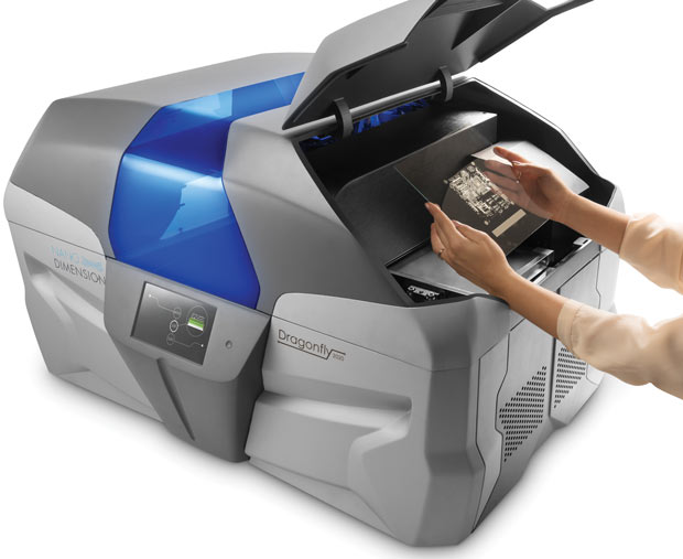
 The Nano Dimension dual-material inkjet DragonFly 2020 3D printer creates professional multi-layer printed circuit boards that include vias, without the need for drilling. The equipment deposits both dielectric and conductive inks and performs an integrated sintering process for curing both materials. Image courtesy of Nano Dimension.
Also exhibiting at CES 2016 was Nano Dimension, a company founded in 2012 that says it is “bringing professional-grade 3D printing to the world of electronics.” Its solution produces true multi-layer PCBs by combining three technologies: DragonFly 2020 3D printer hardware, control software that converts standard Gerber board design files to 3D-printable files, and nanotechnology-based dielectric and metal inks. Silver is in use, and a new copper ink was recently patented. This dual-material system, demonstrated in the U.S. in November at the Printed Electronics USA 2015 conference, creates boards with classic vias (two pads in corresponding positions on different layers of the board that are electrically connected by a hole through the board) as either blind, open or complete paths of conductive material, with no need for drilling.
The DragonFly 2020 deposits 2-micron-thick layers of material, alternating both types within a given layer to create the trace patterns; sintering and curing steps are built in. According to the company’s website FAQs, trace widths are 80-100 microns and build time for a large, complex 10-layer board is several hours. PCBs created with the desktop, office-environment system are suitable for prototyping and one-off projects, bypassing the time needed to work with traditional board services. See a video representation of the 3D printing process:
For More Info
Subscribe to our FREE magazine, FREE email newsletters or both!
Latest News
About the Author
Pamela Waterman worked as Digital Engineering’s contributing editor for two decades. Contact her via .(JavaScript must be enabled to view this email address).
Follow DE

