ANSYS Enhances HFSS for Electromagnetic Simulation
New 3D electrical layout interface and planar Method of Moments solver functionality create highly accurate and automated design flow.
Latest News
May 31, 2013
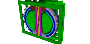
ANSYS recently updated its tool for simulating 3D full-wave electromagnetic fields, HFSS (version 14.5, service pack 2), to include a 3D electrical layout interface as well as a planar Method of Moments (MoM) solver for a more accurate and streamlined design workflow.
The update enables engineers to create electromagnetic simulations using an intuitive layout interface and achieve accurate and high-fidelity results from the HFSS solver. The 3D electrical layout interface also enables more efficient integration with established EDA design flows as well as the direct import of layout geometry from ODB++ compatible databases such as Altium, Cadence, Mentor Graphics and Zuken.
The new planar MoM solver gives users the ability to quickly perform complex calculations and explore design alternatives early in the design cycle while still being able to take advantage of analysis capabilities to optimize and verify the design later in the process. Automatic set up of port assignment, radiation boundary conditions and layered material properties functionalities further simplify the model creation process and allows users to create designs of their electronic products with fully parametric planar stackups, via padstacks and transmissions lines, as well as other types of planar structures and transitions.
“The new 3D electrical layout interface for ANSYS HFSS allows users to easily create fully parametric designs of printed circuit boards, electronic packages and custom integrated circuits from an intuitive interface,” said Larry Williams, director of product management at ANSYS. “This new capability greatly simplifies the model creation process and allows a broad class of engineers to leverage the HFSS solver to extract electromagnetic parameters from critical signal pathways and to explore design alternatives and evaluate design trade-offs prior to fabrication.”
For more information, visit ANSYS.
Sources: Press materials received from the company and additional information gleaned from the company’s website.
Subscribe to our FREE magazine, FREE email newsletters or both!
Latest News
About the Author
DE’s editors contribute news and new product announcements to Digital Engineering.
Press releases may be sent to them via [email protected].


