
An example of a printed circuit board layout. Image courtesy of ANSYS.


Latest News
May 1, 2018
Electromagnetic interference (EMI) and EM compatibility (EMC) have always been key concerns for designers of electrical devices. The RF noise radiates from every electric device, potentially creating internal disruptions or interference with other nearby devices.
Next-generation RF, microwave and millimeter-wave applications like 5G wireless, the internet of things (IoT) and high-speed interconnects have resulted in an increasing interest in EMI simulation. As the IoT expands and embedded electronics become more ubiquitous, it will result in an unprecedented level of co-location scenario complexity.
“It’s expected that 5G will need to utilize higher frequency spectrums in the millimeter-wave range where the quality of the signal can be more vulnerable than the conventional lower frequency applications against the noise from outside the circuit, and the performance can be easily degraded by impedance mismatch, insertion loss and crosstalk,” says Jiyoun Munn, technical product manager of RF, COMSOL Inc.
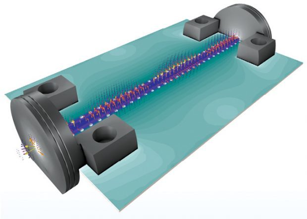 An example of an edge launch connector test circuit board. Image courtesy of COMSOL.
Every connected device can potentially increase the amount of EM radiation and RF noise, and mitigating against the problem with shielding is a costly and complex solution that most companies want to avoid. That means designers will need to engineer that interference out of the devices that they are developing earlier in the process—relying on EM simulation tools to do so.
Buzz Around EMI Simulation
In the past, designers mostly didn’t consider EMI until they presented the finished product for compliance testing. “Then they would go to the anechoic chamber and discover they don’t meet the requirements for radiated emissions, or they are susceptible to internal or external inferences,” says Larry Williams, director of technology at ANSYS. “EMI compliance is a process, and you have to build that process into your design activities. If you wait until the end to see if the product will radiate, you are making a mistake.”
The advent of the IoT and the creation of smaller and smaller electronic components are creating greater opportunities for EMI issues, even in products where this wasn’t previously even a consideration. The cost of mitigating these problems after the fact is a greater concern, particularly when it comes to lower-cost assemblies and products.
IoT devices are smaller and relatively inexpensive, so manufacturers don’t want to spend a lot of money on enclosures and shielding. Components also come from a variety of suppliers, which makes it difficult to manage coexistence or to anticipate how the system will perform in advance.
“You need to do a lot of EM 3D simulation to understand a product well,” says Minoru Ishikawa, market development manager at Mentor Graphics, a Siemens company. “You can have a virtual prototype that helps you identify these issues sooner.”
Simulation software providers have been expanding their EMI simulation capabilities through acquisition. Siemens, for example, acquired EM simulation software company Infolytica, which was folded into the Mentor Graphics mechanical analysis division. Altair acquired FEKO, while Dassault Systèmes acquired CST, a package of tools for EM-centric multiphysics simulation.
Simulation supports designers by allowing them to virtually evaluate several design ideas and implement physical prototypes based on the most promising concepts, as well as investigate different boundary conditions without damaging a prototype.
The goal of simulation specialists is to mimic the real world as closely as possible, so that the prototype is based on numerical results that achieve the expected performance in fewer design and test iterations,” COMSOL’s Munn says.
The difficulty with EMI, though, is that it’s difficult to simulate an entire system. “You’d have to simulate the entire product the same way it would function as when you plug it into a 110v outlet and turn on the power,” says Dave Kohlmeier, senior product line director of Mentor’s HyperLynx product. “There are all of these digital signals and analog signals running concurrently, producing various amounts of radiation in various directions, and it’s almost impossible to recreate that stimulus.”
Kohlmeier says rules-based verification has been used to predict and address the inadvertent antennas created in these systems, an approach that can improve product performance even as the ability to run complex simulation has increased.
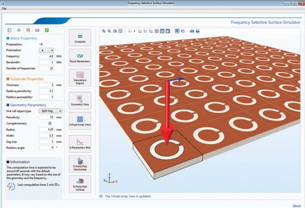 The Frequency Selective Surface Simulator app from COMSOL simulates a user-stipulated periodic structure selected from the built-in unit cell types. Image courtesy of COMSOL.
“That’s especially important in these IoT devices,” says Swagato Chakraborty, director of engineering for HyperLynx Advanced Solvers. “You need to make sure the intended antennas perform correctly, and catch those unintended antennas.”
That activity is difficult to profile. Mentor can simulate the effect of shielding on a given system, for example, but a rules-based approach can help determine where an antenna may have been accidentally created.
“3D simulation can work well when you want to find the optimal geometry or topology, or to understand a path or channel and how to prevent interference,” Kohlmeier says. “Rules-based verification and 3D simulation help each other to develop a good board.”
Smaller Electronics, Bigger Challenges
The fact that electronics components are getting smaller, and being incorporated into smaller products, also poses an EMI challenge. Smaller and embedded electronics are especially prone to challenges involving crosstalk, coupling, interference and impedance mismatching—and adding shielding to these components is more complicated.
“Smaller embedded devices experience the electrothermal effects in an exaggerated manner because of the physical space limitations,” Munn says. “Coupling between devices and signal lines in smaller embedded devices are prone to signal quality degradation due to the impedance mismatching caused by device miniaturization.”
For example, engineers working on high-speed interconnects face a number of design hurdles, as geometry, size and transmission constraints must be met while matching the impedance of the connector to the rest of the transmission line. As the frequency increases, maintaining the impedance becomes more complex, as small quirks arising from the geometry or selected materials can be magnified.
“Analyzing crosstalk is particularly challenging because in situations such as extreme heat or blizzard conditions for example, you now must take into consideration not only the electromagnetic properties, but heat transfer and structural deformation to begin to get an accurate representation of the physics in the real world,” Munn says. “Also keep in mind that the impact of the electrothermal effects will most likely have a much greater impact on a smaller embedded device than it would with a larger piece of equipment.”
EMI issues also often result from signal integrity or power integrity issues—which are also more complicated in smaller devices. “There’s a lot of energy, and it has to go somewhere,” Williams says. “You need good design flow that includes signal and power integrity and that can help reduce EMI problems.”
With smaller electronics, the need for high-speed access to memory and high performance, combined with compressing the electronics into a small space, work against EMI compliance. In the case of ANSYS, the company has built features into its software that can automate and customize design flows around signal and power integrity.
“We’ve built into our tools the ability for engineers to receive a printed circuit board layout and bring those models in, and automate those parts of the process,” Williams says.
A Multiphysics Approach
To successfully miniaturize an electronic product and reduce EMI challenges, engineers need to be able to effectively and efficiently represent the real world as closely as possible. This involves using a multiphysics simulation solution that enables modeling of components and phenomenon that you are not able to physically test in all cases.
COMSOL’s AC/DC Module enables simulation of low-frequency electromagnetics and electromechanical components; the company’s RF Module is designed to model high-frequency EM phenomena and optimize electromagnetics devices such as antennae and micro/millimeter wave circuits.
The AC/DC Module and RF Module can be used for electromagnetic analysis. When this simulation is set up, a user can move on from a single physics electromagnetics analysis and add physics from one of COMSOL’s add-on products, such as the Heat Transfer Module, CFD Module, Structural Mechanics Module, etc.
“Compared to traditional electromagnetic modeling, multiphysics simulation enables the end user to include effects such as temperature fluctuations, structural deformations, and fluid flow to perform virtual prototyping that truly describes the real world,” Munn says.
The ANSYS HFSS simulation tools can be combined via the ANSYS Electronics Desktop to streamline workflows and reduce development time, while rapidly testing and validating EMI and EMC compliance. Engineers can use EMI simulation tools to analyze and optimize trade-offs among speed, bandwidth, signal and power integrity, EMI and thermal performance in these devices.
 ANSYS Icepak is a simulation tool that can perform electrothermal and standalone thermal analyses of electronic designs. Image courtesy of ANSYS.
“If you are putting these electrical devices inside automobiles, you want to know that they are reliable for temperature, vibration and shock,” Williams says. “We can link through the ANSYS Workbench to other tools for thermal, mechanical, structural and vibration simulation and that’s critical.”
Evolving Challenges
As the number of connected devices increases, EMI-related design challenges also will grow. Collaboration across departments and specialties will be important, particularly when it comes to designers who have little or no experience running these simulations.
“When designers are equipped with the right set of tools, they can freely collaborate with colleagues throughout their organization and beyond. Working cross-departmentally will be key to competing and succeeding in the ultracompetitive market we find ourselves in,” Munn says.
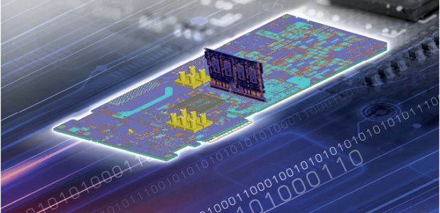 An example of a printed circuit board layout. Image courtesy of ANSYS.
Still, the computational scale required to simulate an entire electrical system would be massive, which is what has made that approach impractical so far. A combination of rules-based verification and multiphysics simulations will be required.
New EMC and EMI models and approaches will need to be developed that take into consideration the greater vulnerability of the IoT, larger concentrations of co-located devices, greater occupation of unlicensed frequency bands and unpredictable and highly dynamic interference scenarios.
Smart devices have to juggle and balance multiple wireless signals, from the Wi-Fi coming from a nearby access point to a GPS signal coming from space. “You have these multiple systems co-existing, and you don’t want the device to destroy its own ability to operate,” Williams says. “Now there are 5G systems coming and high-speed downloads. High frequency is a bigger challenge for designing devices, and having advanced field simulation is key. You can’t cut corners.”
Subscribe to our FREE magazine, FREE email newsletters or both!
Latest News
About the Author
Brian Albright is the editorial director of Digital Engineering. Contact him at [email protected].
Follow DE

