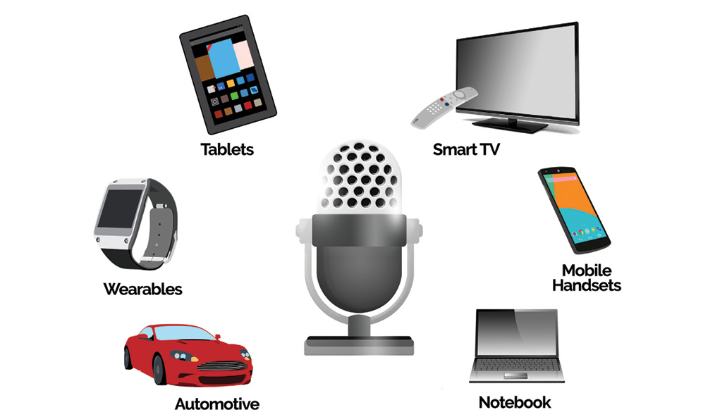
The rise of always-on sensing has opened the door for speech-based interfaces, dramatically changing the way consumers interact with everything from sports watches to automotive control systems. The challenge is: How do you design these systems in such a way that they don’t drain the batteries that power their operation too quickly? Image courtesy of InvenSense.


Latest News
March 1, 2017
New and novel ways of harnessing the power of sensors have begun to redefine the form and function of the latest generation of electronic products, changing the way people interact with and use these devices. Design teams now use terms like “natural,” “interactive” and “hands-free” to describe the man-machine interfaces of sensor-enabled mobile, wearable and Internet of Things (IoT) devices.
A look behind the scenes reveals significant growth in the number, sophistication and variety of the components that allow developers to take full advantage of the information gathered by sensors. Next-generation systems sport a growing variety of specialized processors, large caches, enhanced memory and communication protocols.
 The rise of always-on sensing has opened the door for speech-based interfaces, dramatically changing the way consumers interact with everything from sports watches to automotive control systems. The challenge is: How do you design these systems in such a way that they don’t drain the batteries that power their operation too quickly? Image courtesy of InvenSense.
To get an idea of the scale of this trend, consider Samsung’s Galaxy smartphones. Launched in 2015, the S6 contains three times more sensors than the 2010 Galaxy S. In the same timeframe, the number of processor cores has grown from 1 to 8.
The real change, however, is not the increasing power of sensing and processing resources, but the growing use of always-on sensing to enable voice- and gesture-activated interfaces, as well as context-, environment- or location-aware services. Implementing always-on applications often requires the design engineer to create systems that can operate within the meager power budgets of battery-operated devices.
To address this issue, the design engineer has to do more than reduce the systems’ energy budgets. Slashing power consumption often means sacrificing precision or increasing noise. “Simplistic brute-force approaches of ‘let’s just use a lower power sensor’ may backfire,” says Eitan Medina, vice president of marketing and product management at InvenSense. “Sacrificing performance parameters—such as the noise floor or sensitivity or other parameters—may actually hurt the ability of the [sensor] node to fulfill the end use case or address a portion of the system power that is actually negligible while causing a bigger waste elsewhere.”
A more effective approach calls for tailoring sensor and processor operating parameters to minimize power consumption while ensuring precision measurements. Always-on applications cannot operate on power hungry general-purpose processors running high-level operating systems. The power consumption of these processors is simply prohibitive.
Start with the Big Picture
To effectively address the issues of precision and energy efficiency, engineers should begin their sensor design process by cultivating a deep understanding of the use case on the system level for the end product. “It is always important to see power consumption on the system level and optimize all components to achieve the maximum benefit,” says Jeanne Forget, vice president of global marketing at Bosch Sensortec. “A variety of technologies can have a positive impact on power saving. It depends on the application and use case how much potential can be realized in the specific application.”
Implementing a holistic approach calls for analysis in two areas: architectural analysis and actual measurements. The architectural analysis aims to understand the product’s hardware architecture, identifying the key subsystems and obtaining from vendors as much information regarding the subsystems’ power consumption in each of the key modes to be used by the end product. Once you do that, you come up with a power budget for each of the components in your design.
In the measurement phase, you are looking to correlate actual measurements with your architectural analysis to identify problems and areas best suited for power-optimization. You want to embed in your design prototypes the ability to measure power consumed by the biggest subsystems in the design. This will involve making sure you have test points that allow you to measure current by individual subsystems and chips.
If you have performed these steps correctly, the analysis and measurements will help identify the subsystems and use-case scenarios consuming the most power. You can then seek alternatives to the subsystems that consume the most power.
An example of this approach might involve finding a way to reduce the power required by a sports watch. In this case, the wearable incorporates a GPS system, 6-axis motion sensor and PPG (photoplethysmogram) sensor for measuring heart rate. In this example, the goal is to avoid needing to recharge the watch frequently.
If the primary element that limits the battery’s operating life is the GPS system, then you could turn off the GPS subsystem intermittently, using motion sensors enabled by advanced algorithms to take over navigation functions, delivering a major power reduction on a system level. A side benefit of this holistic approach would be an improvement in the watch’s ability to navigate when the user moves under trees or in an urban environment. If you focus on the components alone and do not adopt a top-down perspective, you can miss possible major power savings and potential expanded use cases.
Implementing this holistic approach requires designers to engage the full spectrum of disciplines, factoring in all aspects of the design. “InvenSense relies on an array of disciplines that work together to identify the right mix that would provide the sensor solution for the end product use case,” says Medina. “The system and software insights influence the hardware and software partitioning of the capabilities and help prioritize tradeoffs in various levels in the sensor design and sometimes in the system design.”
The Discrete Sensor
Working at the most basic level, the design engineer can take several approaches to optimizing the energy efficiency of the discrete sensor. Many development teams begin by fine-tuning the basic power control elements. “We achieve power efficiency through improvements in every element in the discrete sensor, including the sensing chain, drive chain and digital elements such as PLL (phase lock loop), LDO (luminescent dissolved oxygen), and charge-pumps,” says Mahesh Chowdhary, director of strategic platforms and IoT applications for STMicroelectronics.
Optimization efforts also try to eke out energy savings using signal-sampling techniques like compressed sensing, a method of acquiring and reconstructing a signal from far fewer measurements than traditional methods. While this technique can reduce energy consumption, some consider its benefits to be limited. “Compressed sensing is getting a lot of press, but in practical systems, it only provides incremental benefits to energy efficiency,” says Jim Steele, vice president of engineering, intelligent audio, at Knowles Corp. “A system solution with proper duty cycling is the best way to optimize energy consumption.”
 STMicroelctronics LSM6DSM iNEMO inertial module incorporates embedded functions, using hardware blocks to enable such functions as motion detection, tilt detection and step recording. These embedded functions reduce energy consumption by offloading feature computations from the sensor node to the discrete sensor. Image courtesy of STMicroelctronics.
This approach periodically places various subsystems in the sensor system into sleep mode. The lower the duty cycle, the longer subsystems remain asleep, and the more energy they save.
In low-power, always-on applications, duty cycling becomes more complicated. The sensor must run when the system is asleep. This means the system clock is not available. Therefore, the sensor needs an internal clock to run during this time. After an event awakens the rest of the system, the sensor can resume using the system clock.
Duty cycling for this type of application requires a trigger that continuously analyzes incoming sensor data using minimal energy and memory resources, waking up a more powerful processor only when something significant happens. This is where the introduction of advanced software comes into play.
“The idea of duty cycling has been around for a while, but it is being realized now more than ever because more sophisticated algorithms are finding their way into the discrete sensor,” says Steele.
Designers can take the role of software one step further by abstracting relevant context information from the raw sensor data. This opens the door for higher-level algorithms to use the abstracted results rather than the sensor data to obtain additional contextual insights. Adding the abstraction process further reduces the amount of data that must be processed, achieving even greater energy efficiency.
The downside of duty cycling, however, is that it can increase transmission latency and decrease the throughput. As a result, implementing duty cycling requires the design engineer to make tradeoffs between energy efficiency, transmission latency and throughput.
Advocates of duty cycling contend that the best results are achieved by adopting a hierarchical approach. In this technique, lower-power systems trigger successively higher-power systems to meet the required levels of accuracy. To do this, the designer must quantify the power requirements and available accuracy of each subsystem. Armed with this information, the design team can optimize energy efficiency and specify the desired level of accuracy required for the applications with full awareness of the impact of the tradeoffs being made.
Optimizing the Sensor Node
The sensor node presents a more complex arena than the discrete sensor for designers attempting to achieve greater energy efficiency. That said, many of the same techniques and technologies used to optimize the discrete sensor have proven to be relevant to the sensor node.
For example, developing an always-on, energy-efficient architecture for the sensor node also begins with a system-level assessment of the power budgets of the subsystems. As with the discrete sensor, designers can use this analysis to target the most appropriate areas for optimization.
Duty cycling also plays an important role. In the case of the node, this technique can be challenging because of the array of subsystems involved and the complexity of their interactions. Even so, the rewards are significant.
These are a few general practices. Other optimization techniques seek to improve node architectures by specifically focusing on processor and data buffer resources that handle sensor data.
Processor Dexterity
One such approach builds on the principle that the designer cannot afford to run low-power, always-on applications on power-hungry, general-purpose processors running complex, high-level operating systems. This technique advocates developing architectures built on the use of small, low-power, specialized processors that can offload low-level cognitive functions from the general-purpose processor, providing appropriate performance within a sustainable power budget.
“When sensor devices are applied with general-purpose MCUs (microcontroller units), the MCUs often carry significant overhead,” says Forget. “Instead, we [Bosch Sensortec] develop dedicated signal processors for sensor data fusion and sensor algorithms, optimized for the task with respect to instruction set, peripherals and performance. This way, we can achieve a perfectly optimized power budget.”
Complex applications can require a series of processors, with each successive processor handling increasingly difficult functions. For example, a voice-based interface may require a digital signal processor (DSP) tailored for low-power voice detection. Downstream, more powerful processors run advanced voice-recognition algorithms for high-end functions.
Selecting an appropriate processor, however, may be easier said than done. The sheer variety of processing requirements for always-on applications precludes the adoption of a one-size-fits-all approach. There are, though, a few rules of thumb that can help with the selection process. Look for processors with efficient floating-point options for sensor data processing, scalable performance over a range of functionality, and an efficient instruction set with a low cycle count.
A Layered Sensing Approach
Another optimization technique called “cognitive layering” harnesses the power of parallel processing. In a white paper titled “Keeping Always-On Systems On for Low-Energy Internet-of-Things Applications,” Gerard Andrews and Larry Przywara, of Cadence Design Systems, describe a technique of offloading tasks from the general-purpose processor to low-power, always-on DSPs. The idea is to have different layers of a software program run on specialized processors. The lower layers of the software are served by DSPs with just enough processing power to perform the tasks required by the system at a given point.
Andrews and Przywara describe how cognitive layering works using an example of a voice-recognition application on a smartphone. The bottom layer detects noise, which consumes only nanowatts of power. The noise detection triggers a series of actions further up in the processing chain, ranging from detecting a noise to recognizing a command to interpreting the commands in the context of the current application. Thus, each successive level of power consumption is triggered only when it is needed.
The developers of cognitive layering contend that, by using this technique, the designer can achieve optimal energy efficiency while still delivering acceptable latency and throughput. This technique can run on a single chip or include cloud-based processing for more complex applications.
Pushing Functionality to the Sensor
Another approach to optimizing energy efficiency of the sensor node takes the form of shifting more functionality to the discrete sensor. The idea here is that designers can improve performance across the board by beefing up local processing, memory and software assets. Again, the deployment of these resources has to be tailored to meet the specific needs of the use case.
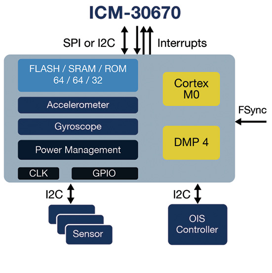 InvenSense’s single-chip ICM-30670 combines gyroscope and accelerometer sensors with an ARM Cortex-M0 CPU and a DMP4 Digital Motion Processor. The specialized processors collect and process data from internal and external sensors, offloading processing from the application processor while reducing system power consumption. The Cortex-M0 CPU provides a programmable platform for software development, and the DMP4 is optimized for fixed-point processing and FFT (fast Fourier transform) generation, offloading math-intensive operations from the main CPU. Image courtesy of InvenSense.
Limited, targeted intelligence plays a prominent role in this strategy. “Knowles is working on improving the energy efficiency of sensor nodes by bring more intelligence into the discrete sensor itself,” says Steele.
This intelligence takes several different forms. For example, Bosch Sensortec sees great potential in local signal processing and buffer memory in the sensor device. “Our sensors have internal FIFOs (first in, first out data buffers) that can be filled with sensor data,” says Forget. “Some of our newer sensors also incorporate additional intelligence inside the sensor, allowing for limited data pre-processing without the need of interacting with the host MCU.
In addition to processors and memory, sensor vendors have expanded local logic by adding embedded functions. “In the sensor node, we reduce energy consumption by offloading some of the feature computation to the discrete sensor,” says Chowdhary. “Discrete sensors from ST have embedded functions such as motion detection, step counting, tilt detection and orientation detection. Implementing these functions on the sensor produces significantly lower power consumption relative to the sensor node.”
A Work in Progress
Growing demand for devices that deliver always-on functionality to support voice- and gesture-based interfaces places great pressure on design engineers to achieve optimum energy efficiency in sensor-enabled devices. While duty cycling, specialized processors, cognitive layering and embedded functions offer designers a variety of ways to reduce energy consumption, it is important to remember that each use case will likely have special requirements and demand its own unique architecture.
While current techniques and technologies have great potential, the coming years promise to bring a new class of design options. It’s safe to say that the drive to build devices that can conveniently operate on battery power is only just beginning.
More Info
Subscribe to our FREE magazine, FREE email newsletters or both!
Latest News


