Fast App: COMSOL’s Multiphysics Enables Quality Control Testing in Semiconductor Manufacturing
The use of the finite element analysis, solver, and simulation software package enabled STMicroelectronics to reduce stresses inside its chips during final testing, resulting in higher reliability of the final product.


February 1, 2010
By Luca Cecchetto, Lucia Zullino And Lorenzo Cerati, STMicroelectronics, Milan, Italy
Semiconductor manufacturers, thanks to technological advances leading to a continuous scaling of lithographic dimensions, are creating integrated circuits (ICs) that are increasingly smaller. Reducing silicon consumption without decreasing device reliability can mean multiple millions of dollars in cost savings. Thus, Pad Over Active (POA) structures have been implemented in most advanced semiconductor technologies to optimize area consumption. With it, active circuitry is designed below test/bonding pads to exploit the interconnection properties of multilayer metal stacks. Simulation with COMSOL Multiphysics allows STMicroelectronics to study these effects and formulate design rules that lead to robust circuits.
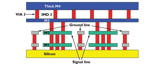 Figure 1. In an IC, circuitry on the silicon layer is connected through metal signal traces (horizontal connects), which in turn are connected to the silicon layer and other metal layers with solid tungsten plugs called vias (vertical connects). (Courtesy of COMSOL.) |
Multilevel Interconnections
In an IC, it’s necessary to carry signals from one subcircuit to another, and for this purpose, a chip uses multiple layers of metal interconnects, each separated by an interlevel dielectric (ILD) layer. Small conductive plugs called vias, often made of tungsten, pass signals from the silicon to a metal layer and also from lower metal layers to the upper one (Figure 1). Further, an IC needs conductive pads on the surface that connect to internal circuitry for two reasons: first, to serve during final manufacturing as spots for the attachment of bondouts, which carry signals from the IC itself to the pins of the final package in which it is mounted and then shipped; second to serve as test points to verify that a device is working properly in what is known as electrical wafer sort (EWS).
“It was only with the COMSOL model that we could determine the areas of peak stress and understand how failures could arise.” |
EWS is conducted on each IC to evaluate its functionality before assembling it in a package and installing it in a final application. The testing is performed by making contact with a pad, using a suitable probe, by lifting the wafer (which is mounted on a chuck) until contact is established with needles inserted in a dedicated card. This condition is considered the reference status (zero level). For smart power ICs, due to the high current levels required and the presence of very precise analog stages, good electrical contact between the needle tip and the pad surface is mandatory. For this reason, an additional overdrive must be applied to the chuck. At the same time, the pressure of the tip on the pad surface must be limited so it does not induce cracks in the ILD layers. Metal extrusion inside of these cracks can, in fact, lead to electrical failures. It is therefore appropriate to investigate and simulate the process to reduce the number of experiments, save time and money, and improve the probe’s design.
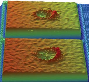 Figure 2. When a probe tip drops down onto a pad with excess force, it creates an uneven surface that can make soldering a bonding pad more difficult. (Courtesy of COMSOL.) | 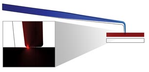 Figure 3. The top plot shows the displacements in the probe and the pad. The white shows the initial contact position, and the colored plot, its final position when the chuck is raised up. The zoomed area shows a plot of the von Mises stresses in the contact area that must be investigated carefully to limit the induced damage. (Courtesy of COMSOL.) |
Probe Design Optimization
One of the most important goals of the EWS process is to limit the induced damage on a restricted surface. The probe tip can scrape the pad surface and create an unevenly shaped crater (Figure 2), and such a wide damaged area does not allow reliable bonding.
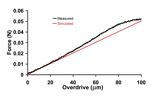 Figure 4. This image shows simulated vertical contact forces versus the applied overdrive compared with the measured forces. The reference position is when the pad first comes in contact with the probe (zero level). (Courtesy of COMSOL.) |
To investigate in detail what happens when a probe tip hits a pad surface, the team at STMicroelectronics decided to use COMSOL Multiphysics, in cooperation with one of its probe suppliers (Technoprobe, Italy). The team was made up of people involved in Technology CAD, POA structures development, and EWS testing inside STMicroelectronics, as well as people dealing with the development of probe cards at Technoprobe. The goals were to validate a COMSOL model with measured data and optimize the probe’s design to increase the performance of the EWS process.
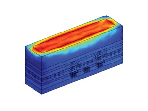 Figure 5. 3D geometry of an IC subsection is used as the basis of a COMSOL model to measure stress in the ILD layers. Shown are the von Mises stresses. (Courtesy of COMSOL.) |
To get the project started, Technoprobe provided STMicroelectronics with a CAD drawing of the current design of the probe, as well as material data. Then, with the help of the Structural Mechanics Module, STMicroelectronics was soon able to develop a 2D mechanical contact model (Figure 3). The results were then compared with measured data (Figure 4). Because comparisons with the results from the model were satisfactory, the team decided to continue to model in 2D and optimize the probe’s design.
The optimization of the probe’s geometry resulted not only in a new and thinner body but also a longer tip. The modified design resulted in better contact between the tip and the pad, less contact force, and a shorter probe mark length. The model and later experiments confirmed that the new configuration provides the equivalent electrical performance with 30% less force.
To improve the pad’s mechanical robustness, a 3D model (Figure 5) of the pad structure and the ILD layout was simulated. Figure 6 plots the von Mises stress in the top ILD for several via pitches. The black line shows the stress without vias, and there are no stress peaks. The other curves show that as spacing gets smaller, stresses rise; the difference between the 1 micrometer and 4 micrometers pitch is roughly 30%. With the model, you can study the number of vias that you can safely put under a POA while still remaining within a safe level of ILD stress. And it was only with the COMSOL model that the team could determine the areas of peak stress and understand how failures could arise.
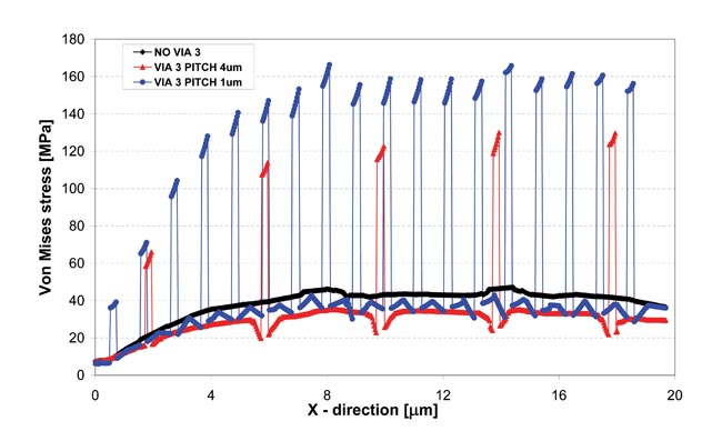 Figure 6. This image shows Von Mises stress in a semiconductor chip inter layer dielectric as a function of via pitch. (Courtesy of COMSOL.) |
More Info
COMSOL
Subscribe to our FREE magazine, FREE email newsletters or both!
About the Author
DE’s editors contribute news and new product announcements to Digital Engineering.
Press releases may be sent to them via [email protected].


