
This app, created from a COMSOL Multiphysics model, computes the diffraction efficiency for reflected and transmitted waves interacting with a wire grating on a dielectric substrate. The app reports the electric field norm plus reflectance and transmittance for a given angle of incidence. Image courtesy of COMSOL.

July 1, 2016
When discussing nanotechnology and simulation, imagine Schrödinger’s cat (or perhaps Alice’s Cheshire version) is peering over your shoulder, pointing out that nanoscale simulation software could approach a problem from the top-down or from the bottom-up, with each way having its pros and cons. One could push current analytical limits down, by scaling existing technologies past those of micro-electromechanical systems (MEMS) devices. Or one could take an upward path, managing atomic and molecular physics in ways that simulate practical, manufacturable devices. Either way, the cats point out, the task involves many factors and application-specific goals that must be carefully considered.
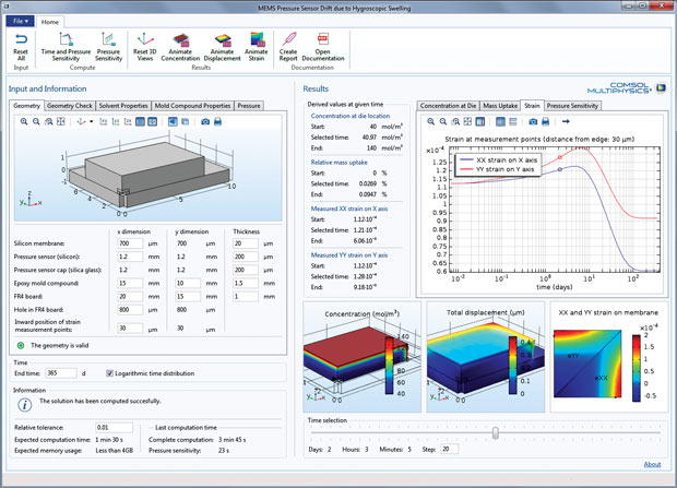 This COMSOL Multiphysics application simulates the drift of measured strain in a MEMS pressure sensor due to hygroscopic swelling. To calculate drift for different scenarios, the user can control the geometric design of the sensor, solvent properties, and material. Image courtesy of COMSOL.
Fortunately, compared to just five years ago (see “Twinkies, Tennis Rackets and Nanotechnology”), simulation tools that take on this task continue to evolve on both commercial and university/consortium fronts. DE takes a look at what you can use right now, with a focus on electrical and mechanical applications.
Commercial Simulation Packages for Nanotechnology
For perspective, SmallTech Consulting, a California firm that provides expert consulting services in several micro- and nano-related technical and business disciplines, offers this general description: “Nanotechnology is the study, design, creation, synthesis, manipulation and application of functional materials, devices and systems through control of matter and energy at the nanometer scale. Further, it entails the exploitation of novel phenomena, including the properties of matter, energy and information at the molecular, atomic and sub-atomic levels.”
With so many possible angles, nanotech-scale computer simulations (sometimes just called modeling) represent a very active field, as evidenced by the ongoing support of the U.S. National Science Foundation (NSF). However a number of companies already offer commercial packages that help designers apply the benefits of nanotechnology to diverse, real-world products.Altair markets FEKO software as part of its HyperWorks suite, supporting the design of such devices as antennas, microstrip circuits and RF components. As a comprehensive electromagnetics (EM) code (including method of moments [MoM]), finite element method (FEM) and frequency- and time-domain finite difference (FD) solvers, FEKO lets users model structures, assign materials/boundary conditions and run simulations all with a sophisticated yet easy-to-use graphical user interface (GUI). One FEKO user is Dejan Filipovic, a professor in the Antenna Research Group in the Department of Electrical Computer and Energy Engineering at the University of Colorado at Boulder, who applies the software to EM analysis of nanowires.
“Modeling nanowires is not an easy task,” says Filipovic, “since the constitutive parameters, specifically complex conductivity, make the system matrix [for computations] poorly conditioned.” However, because the main engine in FEKO uses MoM, “one can set up a problem with many different material wires in arbitrary orientations and still solve it on a desktop. You can study wave propagation including standing waves, coupling and near- and far-fields around these structures to help you better understand the phenomenology.” His group studied impedance, efficiency and patterns for nanowire antennas with FEKO.
COMSOL Multiphysics analysis software has been used for years in a range of relevant applications, from nanoscale heat transfer to nanofluidics to wave optics, supported by one or more add-on modules. Bjorn Sjodin, COMSOL vice president of Product Management, says his company’s software can handle structures down to a bit smaller than 1,000 nanometers, using FEM, finite volume method (FVM), boundary element method (BOM) and particle tracing method. For smaller sizes, he suggests working with software that uses quantum mechanical approaches (not currently offered by COMSOL).
With composite materials so much in the news, current COMSOL user applications stories include: “Buckling Behavior of 3D Randomly Oriented CNT Reinforced Nanocomposite” and “Nanoscale Simulation of Electric Field Enhancement in Polymeric Nanocomposites.” Sjodin notes the latter subject is of interest, because, “although nanocomposites enhance mechanical and thermal properties, they may lower the dielectric strength of a material and make it worse as an insulator.”
Materials Studio software from Dassault Systèmes’ BIOVIA (formerly Accelrys) offers users a modeling/simulation environment to help predict the relationship between a material’s atomic/molecular structure and its macroscale properties. Among the materials the tool handles are catalysts, polymers, composites, metals, batteries and fuel cells. Materials Studio includes a graphical user environment called Materials Studio Visualizer that lets users construct, manipulate and view molecular and mesoscale structures; it is complemented by quantum, classical, mesoscale and statistical solution methods that handle various particle sizes and time scales.
Addressing true atomic-scale modeling of nanostructures is QuantumWise of Copenhagen, Denmark. Founded in 2003, the company has developed a series of numerical analysis tools that go “up to nanoscale” as opposed to having scaled traditional methods “down to nanoscale.” Its products can be used separately or together, typically for semiconductor and electronics applications, though also useful for more general chemical and material simulations. Its tools include Virtual NanoLab (VNL) plus three versions of the Atomistix ToolKit (ATK) for different levels of theory and different scales – ATK-DFT (based on first principles), ATK-SE (semi-empirical approach) and ATK-Classical (classical potential).
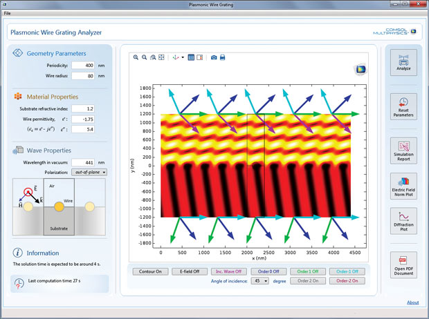 This app, created from a COMSOL Multiphysics model, computes the diffraction efficiency for reflected and transmitted waves interacting with a wire grating on a dielectric substrate. The app reports the electric field norm plus reflectance and transmittance for a given angle of incidence. Image courtesy of COMSOL.
Virtual NanoLab simplifies many tasks within nanotech modeling and simulation, and is extremely helpful for working with structures and data produced in other software. First, it contains an atomic 3D builder tool that reduces user time for setting up and verifying advanced structures. Second, it serves as a GUI (graphical user interface) for all ATK products, supporting easy scripting and results visualization. And third, it works as an interface not only for the ATK packages but also for transferring models to and from other solver codes. All elements have been designed for user efficiency.
This is not an exhaustive discussion of commercial software. Other simulation products exist for targeted applications, such as APSYS (Advanced Physical Models of Semiconductor Devices) from Crosslight and Sentaurus Device from Synopsys, both for semiconductor device design and analysis.
Open-Source Nanotechnology Software
A quick web search for nanotech simulation software immediately turns up the website nanoHUB.org. This organization deserves special mention as a portal for online, free access to more than 400 nanotech-related software programs that run in a browser. The site includes models, courses, datasets, and collaboration tools for working with nanoelectronics, nanophotonics, metamaterials and more, and is operated by the Network for Computational Nanotechnology. Simulation tools (mostly open-source) appear to run as applets but are operated transparently by Purdue University and other grid resources in the cloud.
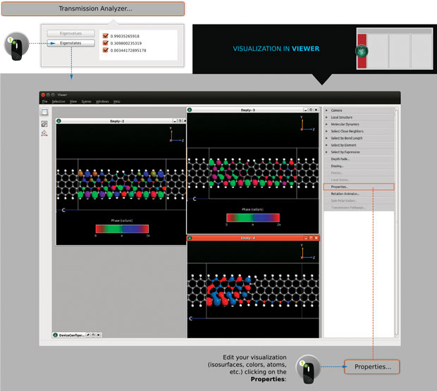 Electronic transport properties through a graphene nanoribbon that includes a distortion, analyzed and visualized with Virtual NanoLab from QuantumWise. Image courtesy of QuantumWise.
Quantum Espresso, overseen by the Quantum Espresso Foundation, is another option. It offers “an integrated suite of open-source computer codes for electronic-structure calculations and materials modeling at the nanoscale.” And, back to semiconductor topics, nano-archimedes is a Technology Computer-Aided Design (TCAD) tool “for the simulation of various technology relevant situations involving the dynamics of electrons such as the transport in nanometer-scale semiconductor devices.”
University, Research Group Activity
Consultancies, universities, government-funded initiatives and online software projects represent the other side of active nano-simulation work. One nanotech-oriented consulting company with more than 30 years’ experience is CFD Research Corporation of Huntsville, AL. It specializes in R&D of computational physics software and applications for government and commercial products, and has already transitioned 20 technologies into the market. CFDRC Technical Fellow Vernon Cole says their most relevant work is in materials modeling, ranging from atomistic and molecular scales up to the fundamental characteristics of microstructures. Much of their work predicts properties and degradation effects of thin films and other coatings.
The new National Nanotechnology Coordinated Infrastructure (NNCI), as announced last September, comprises 16 NSF-funded sites plus a coordinating office (administered out of Georgia Institute of Technology) and will give academic, small business and industry-researchers access to a national network of user facilities. Building on the innovations and discoveries of the National Nanotechnology Infrastructure Network (NNIN), the NNCI involves 27 universities and will include a unified web portal as a user entry point to test equipment, modeling/simulation tools and computational resources.
There are dozens of other universities and consulting groups conducting research to improve nanoscale simulation tools.
At Arizona State University in Tempe, AZ, the work by Dragica Vasileska of the School of Electrical, Computer and Energy Engineering is a stellar example of nanotech research with real-world applications. One project her group has addressed is the ongoing challenge to reduce transistor size. The effort involves investigating self-heating effects. They developed a multi-scale model for thermal transport that balances the energy exchange between electron motion (a particle model) and thermal transport (fluid models involving optical and acoustic phonons), necessary to account for all relevant effects in such nanodevices. Professor Vasileska has also contributed 19 tools to nanoHUB.org, including SCHRED (a self-consistent Schrödinger-Poisson solver) and PREDICTS1D, a tool that simulates copper migration in cadmium-telluride solar cells and the effects on reliability, durability and efficiency.
Besides offering electron-beam lithography, thin film and other fabrication services, the Cornell NanoScale Science and Technology Facility (CNF) also hosts “a diverse suite of simulation tools for nanoscale systems including codes for first principles calculations, photonic devices, molecular dynamics and nanoscale transport.” The facility’s high-performance computing center supports remote access and serves as a software test-bed to ensure code robustness prior to wide-spread distribution.
The University of Michigan Predictive Integrated Structural Materials Science (PRISMS) Center is dedicated to accelerate predictive materials science for structural metals in general, and magnesium in particular. The PRISMS software development program is based on an integrated suite of multiscale/multiphysics computational codes hosted on GitHub. Although these tools are suitable for solving a broad range of analysis tasks, the Center’s focus on metals addresses alloy composition, prediction of tensile properties and calculation of fatigue behavior.
- Altair
- Arizona State University
- CFD Research Corp
- COMSOL
- Cornell NanoScale Science and Technology Facility
- Crosslight
- Dassault Systèmes BIOVIA
- nano-archimedes
- nanoHUB.org
- National Nanotechnology Coordinated Infrastructure
- Quantum Espresso
- QuantumWise
- SmallTech Consulting
- Synopsys
- University of Michigan/PRISMS Center
Subscribe to our FREE magazine, FREE email newsletters or both!
About the Author
Pamela Waterman worked as Digital Engineering’s contributing editor for two decades. Contact her via .(JavaScript must be enabled to view this email address).
Follow DE

