Fig. 1. MEMS mechanisms consist of precisely calibrated, 3D physical structures. To ensure accuracy, layouts must support a comprehensive variety of irregular geometries. Image courtesy of Coventor.

Latest News
March 1, 2016
More on Sensors

It all started with smartphones and airbags. Design engineers began to integrate sensors in growing numbers into such systems to enable smarter performance. These applications mark the prelude to what Alberto Sangiovanni-Vincentelli, a professor at University of California, Berkeley, describes as a “sensory swarm”—a flood of heterogeneous sensors interfacing the cyber and physical worlds. By 2025, experts predict that the swarm could number as many as 7 trillion devices.
One of the first stages in the realization of this sensor-dominated world, the Internet of Things (IoT) requires technologies that can take on smaller form factors and operate on miserly power budgets. In their search to find sensing devices that can meet these requirements, designers have turned to micro-electromechanical systems, or MEMS. Before they can take full advantage of the miniaturization the technology offers and expand its role in the marketplace, engineers must be able to bridge the gaps between the MEMS, analog and digital design worlds. To do this, they will require a new set of tools.
The Devil is in the Differences
Unlike traditional integrated circuit (IC) components, such as resistors and transistors, MEMS mechanisms consist of highly calibrated physical structures (see Fig. 1), such as gears and screws. The difference between these fundamental building blocks translates into two distinct sets of design requirements.
 Fig. 1. MEMS mechanisms consist of precisely calibrated, 3D physical structures. To ensure accuracy, layouts must support a comprehensive variety of irregular geometries. Image courtesy of Coventor.
MEMS layouts must support a broad variety of irregular geometries, unlike conventional IC layout shapes, which usually take the form of rectangles, rectilinear polygons or polygons with 45° edges. Accommodation of these irregular shapes becomes a critical differentiator between MEMS tools and conventional IC tools.
The difference between the two design domains, however, goes beyond the form and shape of the layout elements. Fabrication of these structures requires techniques like surface micro-machining, bulk micro-machining and deep reactive ion etching. In addition, MEMS devices traditionally have been manufactured with processes customized for each device. The variety of these fabrication processes increases production costs and extends the time to market—trends that run counter to the demands of the IoT.
The Crux of the Problem
The elemental differences between the IC and MEMS domains represent the chief hurdle for designers of IoT devices, because by definition these designs require analog/mixed signal, digital and MEMS components to live and function together in one device. Success demands that engineers design these devices with a process that blends all three domains, ensuring that they work well together, whether they reside on a single chip or multiple dies.
Designing for Packaging
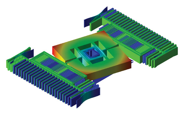
As the “sensory swarm” and the IoT increase pressure on MEMS design automation providers to enable greater levels of multi-technology integration, packaging increasingly affects the performance of the overall system. A good example of MEMS packaging effects can be seen in capacitive MEMS accelerometers and gyroscopes. These devices are relatively large—hundreds of microns across—and quite flexible, and they are attached to the substrate at a small number of points called anchors. Changes in ambient temperature cause the substrate to warp, which in turn causes tiny but detectable changes in the output capacitance of the sensor.
Design tools must be able to accurately predict these miniscule effects so that designers can mitigate their impact or at least know whether the resulting design will perform within specifications (see Fig. 5). MEMS and CMOS tools should interoperate with specialized packaging tools and interface with models provided by package vendors.
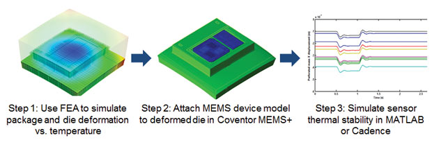 Fig. 5. This composite image depicts a methodology for predicting packaging effects on a MEMS inertial sensor. Image courtesy of Coventor.
As market pressure drives the integration of MEMS devices into high-volume complementary metal oxide semiconductor (CMOS) IC manufacturing, MEMS providers must find ways to shorten development time, reduce costs and deliver increasingly complex performance and greater reliability. Incorporating MEMS design directly into the CMOS design flow provides the most efficient way to achieve this goal, but this will take some work on the part of MEMS design tool providers because the gulf between the two domains remains significant.
“The current design practice at many MEMS industry leaders still involves disparate tools for MEMS and CMOS design,” says Steve Breit, vice president of Engineering at Coventor. “MEMS designers rely on conventional finite element analysis (FEA) tools to do their design, while CMOS designers rely on electronic design automation (EDA) tools. There is no automatic bridge between FEA and EDA tools. MEMS designers spend lots of time and expertise manually creating behavioral models for the CMOS designers. With all the manual effort, it’s easy to introduce errors or for models used by CMOS designers to get out of sync with an evolving design.”
Greater integration of the two design environments is needed. MEMS designers must be able to share design databases, models and results with CMOS colleagues and analyze the interactions between the two technologies. They also have to be able to maintain design database integrity and communicate design data across a variety of tools. For example, MEMS designers should be able to pass data directly from the CMOS layout environment to emulation and simulation tools, maintaining design integrity so that they simulate what they build.
“I would call it a MEMS-CMOS co-design flow,” says Mary Ann Maher, CEO of SoftMEMS. “A tool suite can be constructed that allows MEMS and CMOS designers to use the same tools, but their flow through those tools may be different, and the MEMS designers may use some tools not used by the CMOS designers and vice versa.”
One of the steps required to achieve this co-design flow is to enable MEMS designers to easily create or export models compatible with commonly used environments like MATLAB, Simulink and Cadence Virtuoso. “That is not the case today for MEMS designers who use conventional FEA tools with proprietary solvers to simulate their designs,” says Breit. “The common practice is to handcraft a behavioral model that runs in the system and circuit design environments based on expert physical insight. Hand-crafted models are often over simplified and quickly get out of sync with the design.”
Integrating the design flows of these two disparate domains calls for a more structured strategy. “A structured flow will help you use a top-down design process, where you can focus more on optimizing the complete system instead of optimizing the individual components of the design,” says Nicholas Williams, product marketing manager for Mentor Graphics.
This structure can also take the form of standardization, which many aspects of MEMS design lack. “A structured design flow can take advantage of standard rules and design checks in an organized manner that prevents mistakes and overall can take less time,” says Maher.
MEMS Building Blocks
One way MEMS design automation providers promote standardization is by providing libraries of proven, physical and scalable parameterized primitives, as well as test structures and packages (see Fig. 2). Each primitive should have an underlying model that captures mechanical and electrical physical behavior. The library’s primitive models should support multiple simulators—such as SPICE, Verilog, MATLAB and 3D analysis—and different simulation types, including transient, frequency domain, optimization as well as noise and statistical analyses. These models must simulate fast enough to provide for design optimization and manufacturability studies.
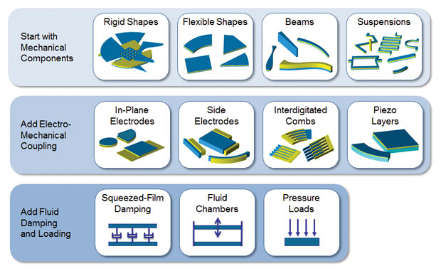 Fig. 2. Just as IC designers use SPICE model libraries to assemble electronic circuits, MEMS engineers rely on component libraries for physical primitives to create layouts. These building blocks include an underlying model that captures the mechanical and electrical physical behavior of the mechanism. Image courtesy of Coventor.
Much like IC designers assemble an electronic circuit by selecting components and building models from a SPICE model library, MEMS designers select fabrication-ready components from the library, define parameters (e.g., length, radius and thickness), and assemble them in a layout, significantly reducing the design process. The designer can also use the library to supply material properties to simulations.
“The MEMS component library should be constrained by the process technology, but flexible enough to describe a wide range of complex, real-world MEMS sensors,” says Breit. “Users should be able to create sensor models that are parametric with respect to key design, manufacturing and environment variables. The model must also include physical effects, such as electrostatic fringing fields and gas damping, and nonlinear effects such as electrostatic and mechanical nonlinearities.” (See Fig. 3.)
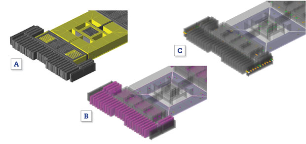 Fig. 3. Shown here are multiple views of a MEMS device, depicting (a) a solid component view, (b) an electrical view and (c) a mechanical view of a 3-axis MEMS gyroscope. Image courtesy of Coventor.
Visualization also plays a key role. “The component library should provide multiple views of a device at various levels of abstraction, ranging from schematics, multiple simulation views, layout, layout abstract, 3D geometry and mesh views if appropriate,” says Maher. (See Fig. 4.)
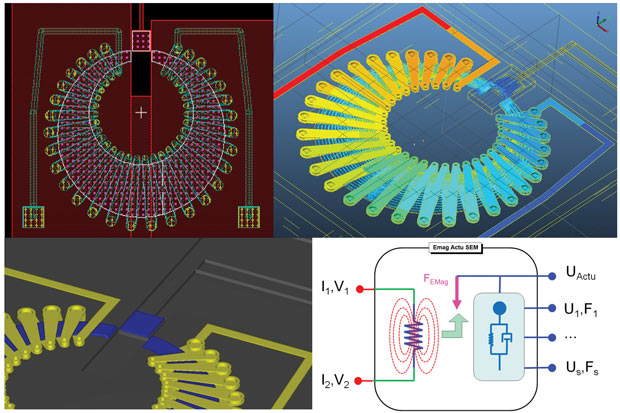 Fig. 4. A design platform should support multiple views of a MEMS or IC device at various levels of abstraction, ranging from schematics to 3D geometry and mesh views. IC and MEMS designers should be able to share these views to ensure design integrity. Image courtesy of SoftMEMS/Mentor Graphics.
Design Glitches and Fixes
Problems can occur even when engineers assemble a design using the predefined building blocks of a component library. Some complications arise if the complex geometries of the components have not been handled correctly.
For example, MEMS layouts can contain curvilinear shapes, and these shapes should be correctly translated to mask output formats. Designers should be able to specify and manipulate curves in a natural way with direct curve representations, using intelligent methods that ensure that curves get approximated as all-angle edges to improve accuracy. Designers should be able to pass curves to process emulation tools in a direct curve representation for interpretation and meshing as opposed to a polygon format, which may not be the correct discretization size for efficient meshing. Also, design environments should provide a method of creating a hierarchy of different parts of the MEMS design to make it easier to assemble symmetrical MEMS devices.
Another area of the design process that can create problems lies at the point where design and manufacturability meet. Designers usually have multiple ways to construct a sensor model, and some construction approaches result in models that violate physical design rules or provide inaccurate simulation results.
“To reduce or avoid these issues, the design environment should provide a way to impose manufacturing and design constraints,” says Breit. “For a given manufacturing process, some components may be excluded from the [component] library, and material properties, process parameters and geometric parameters of the remaining components may be constrained.”
One solution is to select a design environment that offers a customizable component library. This provides a platform for creating MEMS process design kits that help ensure that the resulting designs can be manufactured and will behave as the designers expect.
Getting It Right
IC designers typically use a layout vs. schematic comparison and design rule checking (DRC) for physical verification. For MEMS devices, however, verification requires designers to depart from traditional IC verification techniques. MEMS designers also must perform DRC to confirm a design’s manufacturability, but component structures typically have curved geometries and a variety of all-angled layouts, differing significantly from traditional IC designs.
As a result, MEMS designers must perform physical verification for the entire die, requiring two or more design sources that go into the complete die layout. One design source could be the layout of the active MEMS, generated from a MEMS component library or by a tool that supports true curves and all angles. The other design source could be the inactive parts of the design, such as interconnect wiring and bond pads, created in an electronic design automation (EDA) tool such as Cadence Virtuoso. The environment should automate, as much as possible, the combination of these two layout sources into a single layout that can be sent to an established DRC tool, such as Mentor Graphics’ Caliber.
DRC should encompass manufacturing, context-sensitive and device-specific rules. Additionally, the technology should be able to handle curved structures efficiently without false errors.
“You need the ability to filter out false DRC violations that typically arise from DRC rules written for orthogonal layout,” says Mentor Graphics’ Williams. The ability to remove edges that don’t project or only overlap by a small amount helps to remove false violations due to all-angle, curved edges and round-off. When a curved edge is approximated by multiple small edges, typical checks that assume a single edge intersects both sides of a box break down and cause false violations. This typically occurs in an extension check. The small edges that get created and don’t intersect with the other layer can have reasonable projection lengths and, as a result, will not be filtered out based on projection. This can be handled by saving the results of an extension check as a polygon and checking the internal width of opposite or near opposite edges only.
While these practices have proven to be key elements of the verification and DRC processes, they represent the tip of a larger, more complex challenge. Increasingly, 3D modeling plays an important role in design verification.
Moving Forward
Over the next five years, MEMS design automation providers will focus their efforts on bringing the design process more in line with high-volume, consumer product delivery demands while enabling greater multi-technology integration. “We will see more and more design re-use tools to reduce time to market with design kits, libraries and IP (intellectual property) tools for proven designs on proven processes,” says Maher. “But at the same time, we will see tools to manage the design of devices using new materials and manufacturing processes, as device designers take advantage of flexible materials, low-cost substrates and printed devices.”
As MEMS play a broader role in the marketplace, you will see design environments tailored for IoT designers who may not have MEMS experience, allowing them to use off-the-shelf parts to design systems. “There will be MEMS PDKs [process development kits] based on the MEMS component library approach available from independent foundries for proven MEMS processes,” says Coventor’s Breit. “We don’t expect the IoT device designers to delve into detailed MEMS design, but rather to customize reference designs to suit their needs. The MEMS PDKs will make it much easier to customize and integrate MEMS and CMOS at the package and wafer levels.”
For MEMS designers, the component library approach will continue to evolve to address more complex designs and advanced physical effects. The libraries will provide automated links with front- and back-end layout tools. On the front end, it will be easier to import a MEMS layout and construct a MEMS model. On the back end, the level of automation for combining active and inactive portions of the die layout will improve. There will also be advances in automated design optimization and manufacturing sensitivity studies, enabled by widespread availability of powerful computing resources through public and private cloud computing.
More Info
Subscribe to our FREE magazine, FREE email newsletters or both!
Latest News


